|
STARTSEITEN |
||||||||||||||
|
|
||||||||||||||
|
|
||||||||||||||
|
>>>Links: |
 |
|
Room plant works as DVB-Television- antenna DVB-terristrical-television is becoming more and more popular. The digitalized TV-signal can be received very perfectly even with little room antennas. If one dont want to use a technical device as an antenna, a room plant can be used instead as antenna to receive DVB. The plant to be used is the popular dieffenbachia. (dont touch the sap of this plant).The plant is used as an lambda series resonator with L-coupling: Requirements:
The connection of the plant:
|
|
Insulated and potential free DC-current measurement using magnetics Here is a relatively simple circuit to measure insulated DC currents without any DC- loss. Examples for this requirement are:
The primary circuit: We use the well known DC-current measurement method, where a DC current changes the inductance of a coil wound on a core having a hysteresis. The core must be dimensioned in such a way , to change the hysteresis by means of the DC current to be measured flowing only trough one up to three windings on the core. If the temperature never changes and each core would have exactly the same hysteresis , the development would be very simple. But its not the case. We solve this two problems using a feedback circuit witch cancels all unlinearity and outside influences. The circuit used is shown in Fig.1 . We see two controlled inductances. K1 and K2. Each inductance is connected to a AC voltage to be divided by the inductances. K1 is controlled from the measurement current I1 whereas K2 is controlled by an feedback current having a proportional value of I1.The difference DV of the DC voltage from both dividers is amplified and leaded back to K2. Its obvious, DV is kept constant in this circuit even if the core constants or the temperature changes. Fig.2 shows, the loop equations.
Fig.1 Potential free DC-current measurement.
Fig.2 Equations to DC-measurement
|
||||||||||||||||||||||||||||||||||||||||||||||||||||||
|
Some broadband transformers using twisted wires 1.0 Basics Broadband transformers to be used in RF-circuits often are build as twisted line transformers where the line is wound around a high permeable ferrite core.The possible transformer ratio is 1. Fig.1 shows the mechanical arrangement on a ferrite bead. Such devices work at 2 Principes: #1: At lower band end the transformer works as usual device where the primary inductance certain's the band end frequency fu. Fig.2 shows, the cut off frequency circuit and formula.
Fig 1 Basic transformer #2: At upper band end the transformer works as a line transformer. The ferrite core has no electrical function at band end.The length and the Z of the 2-wireline are the important parameters here. The usual tangents function of 2 pi / lambda is valid here.The transformed Z is : At the length of quarter lambda the well known transformation formula is :
The frequencies between #1 and #2 is the crossing range . Practical transformers never had insertion-loss-ripple there. The crossing of the working ranges is smoothly. The impedance of the wires at Fig.1 depend on the thickness of the copper core, the isolation, and the distance between the wires. It is obvious, that this impedance is unstable. A better practical solution is to twist the 2 wires. The impedance depends here on the number of twists per length. Table 1 shows the impedance of several twisted wires. Tab.1 The impedance of twisted wires
2.0 The auto transformer An other circuit allows an impedance ratio of 4. Fig.3 shows the basic circuit of this twisted wire auto transformer. If
the used wire has an impedance of Zl = 2Z, the output impedance will be 4Z. For the lowerfrequencys , the above
shown formulas are valid.The upper frequency depends on the on the core dimension and wire. The solution then will
be always a compromise between core size and lowest frequency and bandwidth. Fig.4 shows the formulas for the upper frequency
Fig. 4 Fig3. Broadband auto transformer Practical devices of this type my span 3 decades. 3.0 Variable ratios Up to now , we could realize the ratios of 1 and 4 .To match practical circuits , different ratios are necessary. This can be reached in mixing normal design with broadband design. Fig.4 shows this solution having a Z-ratio of 2. As the single winding N3 has low coupling, we must compensate the stray inducdance using a series resonator Cs and Ls. The data is:
Fig.4 transformer having a variable ratio
Super broadband transformer matches bit rates In high bit rate digital communication systems, components having very broad band transmission are necessary. If we imagine that one bite must not be flattened and make an fourier analysis of one bit, the necessary upper frequency must be about10 times the bit rate . As bit rates my vary from khz to Mhz range a band with from khz to Mhz are necessary in a universal digital modem.The necessary input transformer must therefore cover 4 decades. This values can be reached , using 4 twisted wires, one of them is N3 of Fig.5. but is shorted into the twisting.The series resonator is build inside the transformers windings as Fig.5 shows. The data is:
Fig.5,6 Super performance transformer
|
||||||||||||||||||||||||||||||||||||||||||||||||||||||
|
DD circuit linearizes PCB Roll off Due off unavoidable parasistics, RF circuits on PCBs are deteriorated by a roll off up to 1dB. A simple circuit can linearize this roll off. The DD-circuit was developed at the latter days of analog feedback design to differentiate (DD) the signal getting better time behavior, but we will use it as linearizing circuit. Fig.1. Shows a T-circuit having a certain impedance, which is bridged by two capacitors.
Fig. 1 DD circuit The transmission of this circuit depends on its matched Z. Therefore, the reflection coefficients(S11,S22) of the connected devices, must not below 15dB.The Transmission is:
We see 2 corner frequencies producing +20 dB per decade and a -40 dB corner frequency. Adjusting the damping of this corner frequency and the corner frequencies, the circuit can be either a linear, a parable or a ripple function. Fig.1
fig. 2 S12, S11, DD circuit using C1= C2 =15 pF; R1 = R2 = 12 Ohm; R3 =100 Ohm
|
|
The Noise Threshold of PLL -FM-Demodulators PLL FM Demodulators are widely used in communications receivers, because of its low noise threshold. Below this threshold the demodulator noise will
increase drastically. Fig.1 shows the typical Input Signal to Noise Ratio versus Output Signal to Noise Ratio diagram of an PLL- FM- Demodulator. Fig.1 Typical noise Threshold of a PLL - FM-Demodulator A very good value of the threshold TS is 6dB.The threshold formula shows, that lower values are difficult to develop. The threshold TS is :
From this Formula, it is obvious, the threshold only can be optimized , by increasing PLL bandwidth and speed. Only using a high order loop will increase PLL speed. |
|
An high order PLL, to be used as an FM-Demodulator, must be made faster than the simple ones. The earning of the bigger bandwidth leads to higher signal sensitivity . In the Literature, one can find first order and second order loop PLLs. But this circuits are limited especially in the bandwidth of the PLL at the upper bandend. In this demodulator application, the parasitics of a PCB will decrease the bandwidth. A way out of this problem is to use high-order filters and increase the total order of the PLL in producing extra phase for loop stability. Fig.1 shows the discriminator circuit. Fin is the FM modulated carrier. The demodulated video signal then appears as Vout.
Fig. 1 PLL
Fig.2 The high order loop filter
The well known equations for the open loop are: Gain = Kv*Ph(s)*F(s) *PCP(s) .The parasitic of component connections lead to a roll-off PCB(S), this roll off must be compensated by means of the filter :
As Fig.1 shows, there is always a low pass of the PCB layout in the signal path. To minimize this parsitics, the best layout of the PLL is a sandwich of two small PCBs where the feedback signal flow is in the opposite direction than the main signal . Fig.3. Fig.4 shows the open loop Nyqiustdaiagram . The zero crossing frequency of the gain is at a frequency of 90 Mhz .Using this Bandwidth, the PLL will demodulate a video signal with a better threshold value than an smaller PLL: The datas are :
Fig. 4 Open loop Nyquistdiagram of a Fast PLL
|
||||||||
|
AGC-Amplifiers to be used for RF or IF application , have a certain DC- controlled gain range. In this range the amplifier works linear and no distortion must be expected. But to get high RF-power at the output, a power stage has to be added . In this case, the controlled gain rage is limited by the saturation of the RF-amplifier , Fig.1. This limitation will cause intermodulation products especially at multi carrier operation. Do avoid this signal distortions, the amplifier must not work at a working point above 3 db below saturation. Fig.1. This requirement limits the regulation range for the incoming unstable RF signal. With a simple linearisation circuit , the regulation range can be enlarged a lot. The function is as follows:
Fig.1 Power amp. Fig.2 Two AGC-amps Fig.3 Total-circuit
Fig.4 New RF-AGC
|
||||||||
|
Some RF circuits for instance oscillators, are very sensitive to DC supply variations. This circuits need a DC Voltage of 0,1 % instead the usual 1%. A simple pre regulator solves the problem. Fig.1 shows the circuit. The values of the transistors depend on the main current and the beta of the transistors.The Zener voltage must be selected for maximum stability. The main transistor may be very small, if the big filter capacitors are on the input of the pre regulator to avoid big inrush currents . Fig.1 DC Preregulator |
||||||||
|
Spreadspectrum AKF has 4 bit range In the telecommunication code multiplex technology, the modulated signal is spread with a codeword. This technique is called spread spectrum. (SPRSP). In a SPRSP receiver the code word must be found and looked to be received. Fig. 1 shows a standard delay look loop to be locked to the code word which has a certain length, for instance 256 bit. We see here a code generator to generate a certain codeword.The code generator is shifted in its phase from a voltage controlled oscillator to be locked in with the incoming, code word. If they coincide, the loop is looked.The shifting of the code word versus the incoming code word has a control AKF-funktion of Fig.2 The linear look-in control range of the feedback is plus minus 1 bite.Outside this control function the loop may flip out and the signal path is interrupted. In Fig. 3 is a new AKF-Loop shown where the lock-in range is twice. The total lock in process is now easier and faster.This broader AKF is reached by summarizing the output voltages of the detector instead of subtracting them and switch the code generator periodically plus minus one bit.
|
||||||||
|
The distribution of RF power in circuits is normal.To realize this power splitting, a lot of practical couplers, dividers ,and splitters are on the market. But at broadband circuits for digital communications their specification are not precise enough. S21 Transmission specification in RF circuits for digital communication are very tight , ripples and roll off must be below 0.1 dB. For instance , the sinx/x increase for digital radio modulator is only 0.5 dB absolute. Look at: Link >>> Go to digital radio modulator A simple active splitter can divide Power very precisely. Look at Fig. 1 where a Doubel-T resistor network is used. An RF. -OP-AMP amplifies the divided power.This splitter may split the signal to a intermodulation feedback system.
The datas are:
|
||||||||
|
At the old RF Circuits, we matched different components, circuits and amplifiers by designing complicated lumped LC-circuits by means of the smith chart, to not loss any gain of the circuit. As Gain is not the problem any more, due of integrated RF Amplifiers, matching philosophy can be changed to resistive compulsory matching. That means, amplifiers and circuits are connected using a regular resistive network having some gain loss. This loss then is compensated by using one or two more amplifiers. The advantage of this method is the total saving of matching-adjustment manpower. But sometimes intermodulation products my be a problem and must be calculated.. Now, remember the resistor networks to be used for matching :
Where alpha is the damping (Neper ). 1 Neper = 8,6859dB
|
||||||||
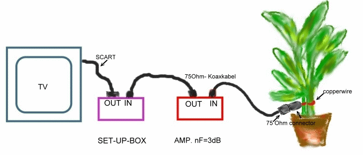
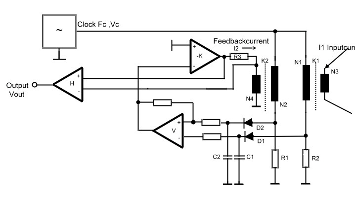
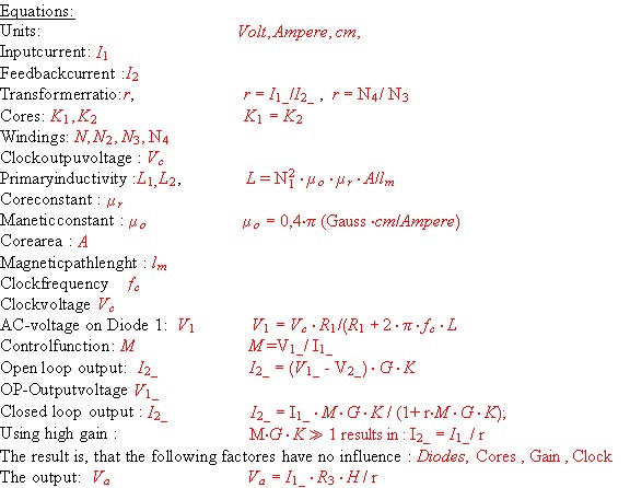

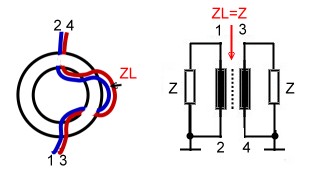 Fig.2 The lower band end

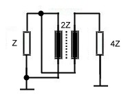
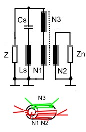

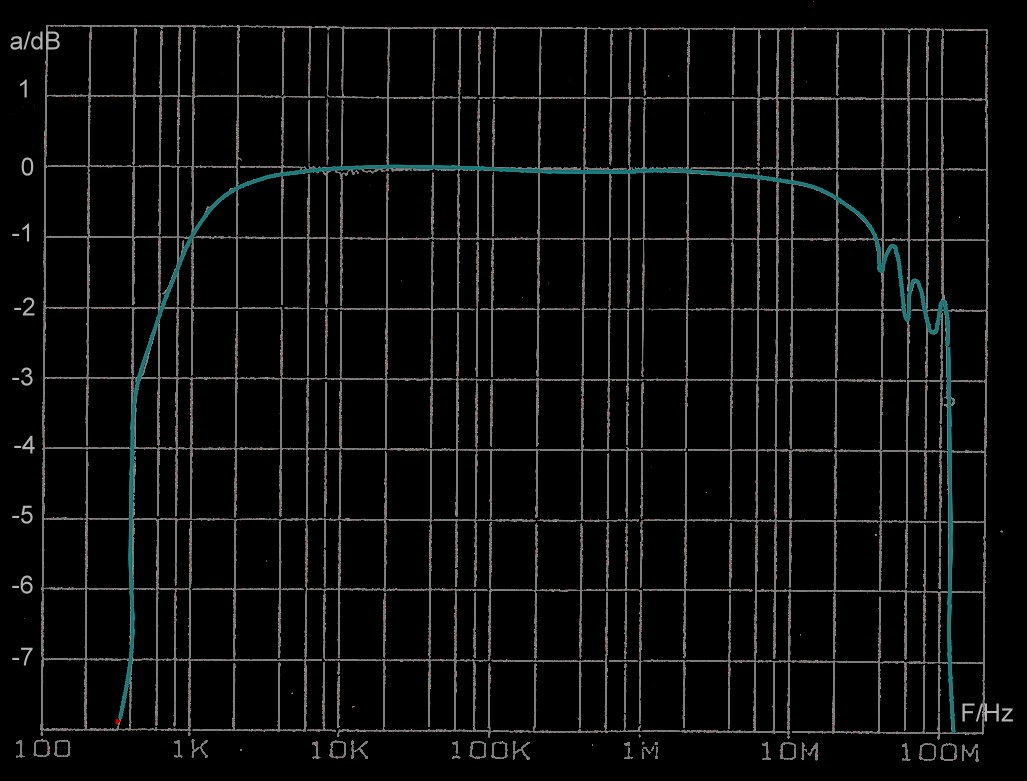
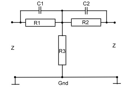
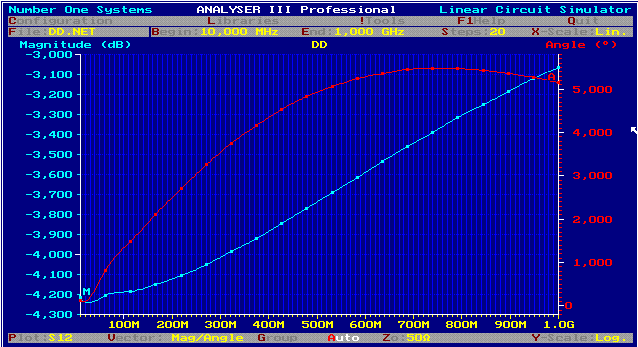
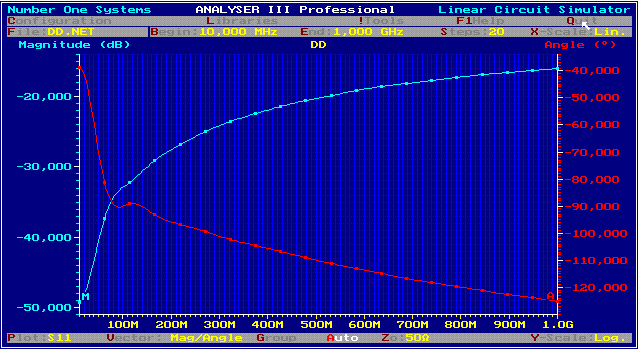
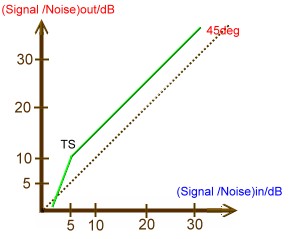
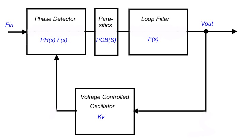
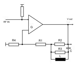

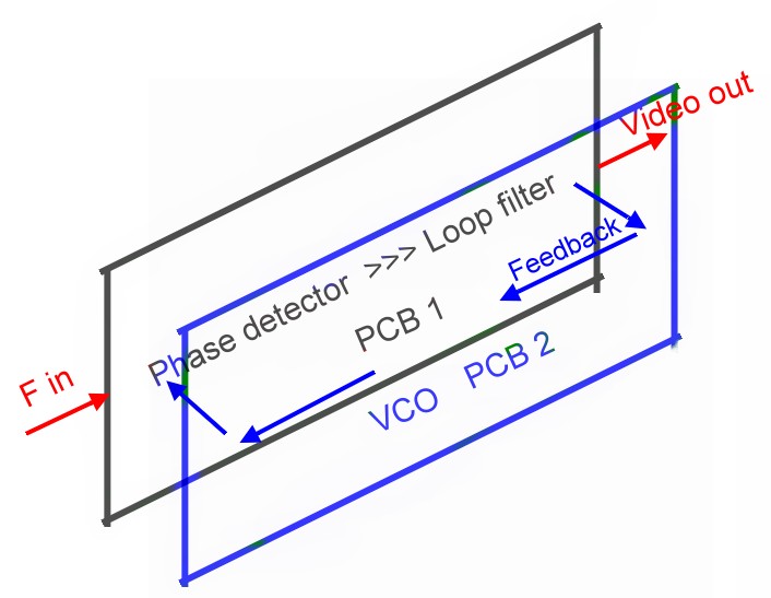
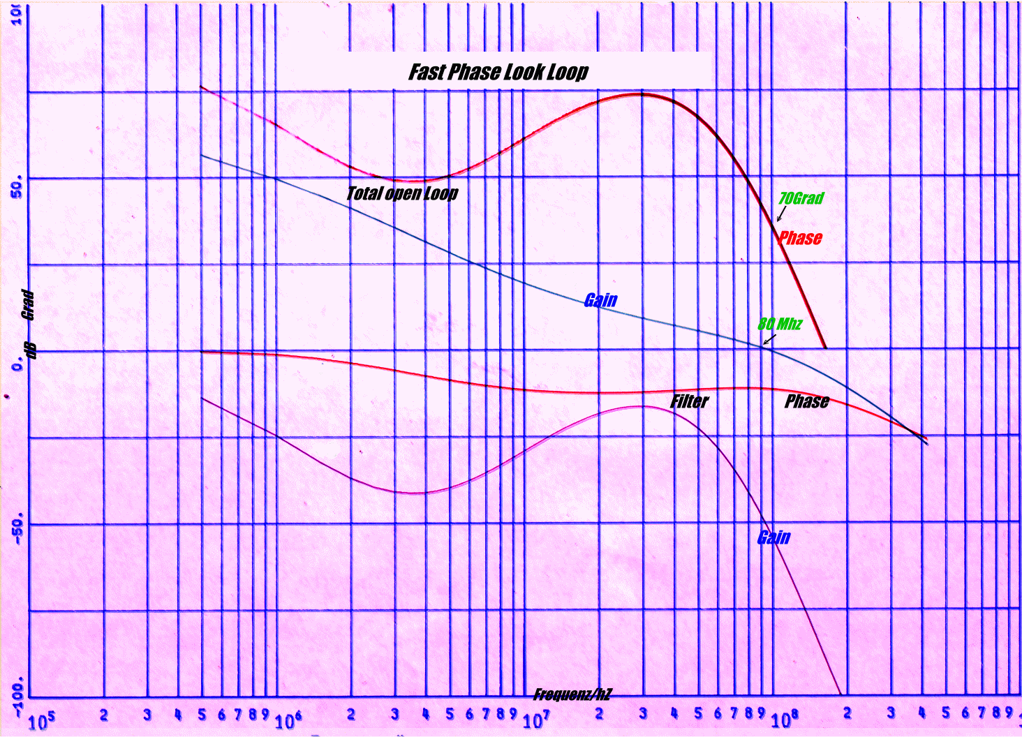
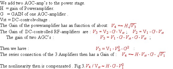
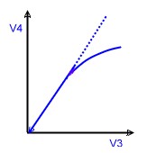
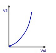
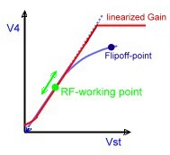
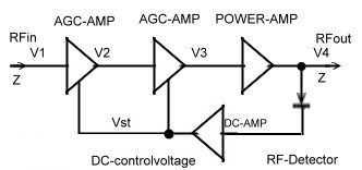
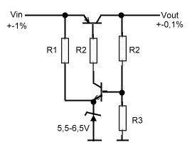
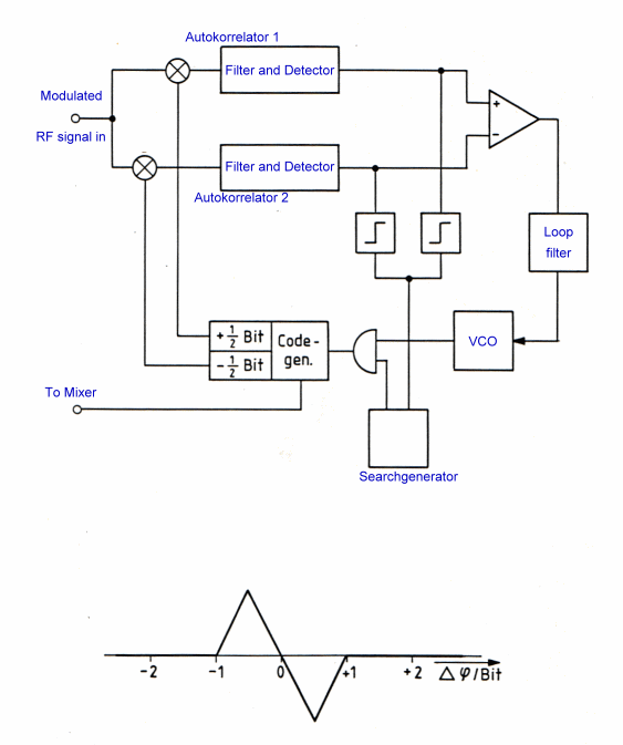
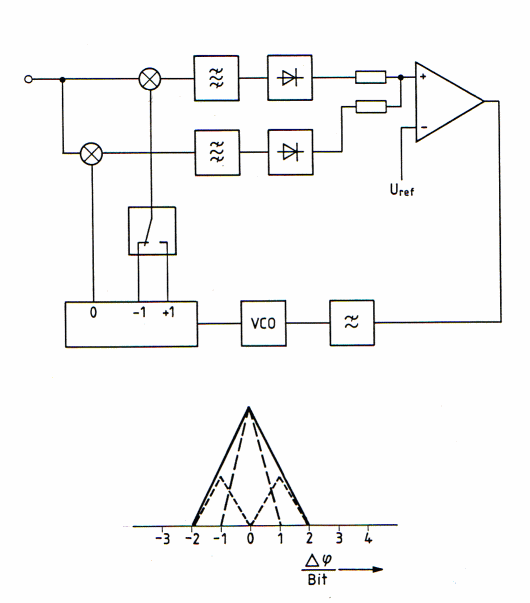
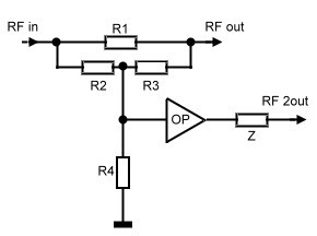 Fig.1 Active 50 Ohm splitter.

